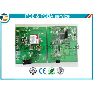
4 Layer PCB Prototype 94v0 PCB Board Surface Mount Prototype Board
andnbsp;
andnbsp;
Production Introduction
Layers andnbsp;: 4 layerandnbsp;
Size : 100mm* 65mmandnbsp;
Material : FR4
Surface Treatment: Lead Free HASL
Board thickness : 1.6mmandnbsp;
Copper thickness: 1ozandnbsp;
Solder mask color: Greenandnbsp;
Silkscreen color: Whiteandnbsp;
Blind and Buried Via: Yesandnbsp;
andnbsp;
andnbsp;
Technical Capacity of PCB Manufacturingandnbsp;
andnbsp;
| Item | Mass Production | Pilot Run Production |
| Capacity | Capacity |
| Layer Counts | 1Landmdash;18L, HDI | 20-28 , HDI |
| Material | CME1,CME3,FR-4, High TG FR4 , Halogen-free FR4 , aluminiumandnbsp;,Ceramic(96% Alumina) |
| Teflon,PTFE(F4B,F4BK), Rogers(4003,4350,5880)Taconic(TLX-8,TLX-9), Arlon(35N,85N)etc. |
| Material Mixed Laminate | 4 layers -- 10 layers | 12 layers |
| FR4+Ro4350 , FR4+Aluminium , FR4+ FPC |
| Maximum Size | 610mm X 1200mm | 1200 - 2000MM |
| Board Outline Tolerance | andplusmn;0.15mm | andplusmn;0.10mm |
| Board Thickness | 0.125mm--6.00mm | 0.1mm--8.00mm |
| Thickness Tolerance ( tandge;0.8mm) | andplusmn; 8% | andplusmn;5% |
| Thickness Tolerance( tandlt;0.8mm) | andplusmn;10% | andplusmn;8% |
| Minimum Line / Space | 0.10mm | 0.075mm |
| Trace width Tolerance | 15%-20% | 10% |
| Minimum Drilling Hole (Mechanical) | 0.2mm | 0.15mm |
| Minimum laser hole | 0.1mm | 0.075mm |
| Hole Position/hole Tolerance | andplusmn;0.05mmandnbsp;andnbsp;andnbsp;andnbsp;andnbsp;andnbsp;andnbsp;andnbsp;andnbsp;andnbsp;andnbsp;PTH:andplusmn;0.076MMandnbsp;andnbsp;andnbsp;andnbsp;andnbsp;NPTH:andplusmn;0.05mm |
| Mini hole ring (single | 0.075MM | 0.05MM |
| OutLayer Copper Thickness | 17um--175um | 175um--210um |
| InnerLayer Copper Thickness | 17um--175um | 175um--210um |
| Mini Solder Mask Bridge | 0.05mm | 0.025mm |
| Impedance Control Tolerance | andplusmn;10% | andplusmn;5% |
| Surface Finishing | HASL, Lead free HASL, Immersion gold, Immersion tin, Immersion Silver. |
| Plated gold , OSP, Carbon ink, |
| 1-2L Lead-time | 3-7 days | 1-2 days |
| 4- 8L Lead-time | 7-10 days | 2-7 days |
| 10-18L Lead-time | 10-15 days | 4-9 days |
| 20-28Landnbsp;Lead-time | 15-20 days |
| Acceptable File Format | ALL Gerber Files,POWERPCB,PROTEL,PADS2000,CAD,AUTOCAD,ORCAD,P-CAD,CAM-350,CAM2000 etc. |
| Quality Standards | IPC-A-600F and MIL-STD-105D CHINA GBandlt;4588andgt; |
andnbsp;
andnbsp;
Technical requirement:
1) Professional Surface-mounting and Through-hole soldering Technology
2) Various sizes like 1206,0805,0603 components SMT technology
3) ICT(In Circuit Test),FCT(Functional Circuit Test) technology.
4) PCB Assembly With UL,CE, FCC, Rohs Approval
5) Nitrogen gas reflow soldering technology for SMT.
6) High Standard SMTandamp; Solder Assembly Line
7) High density interconnected board placement technology capacity.
andnbsp;
andnbsp;
PCB or PCB Assembly files requestsandnbsp;
1) Gerber files of the PCB Boardandnbsp;
2) BOM(Bill of material) for assemblyandnbsp;
To short the lead time, please kindly advertise us if there is any acceptable components substitution.andnbsp;
3) Testing method andamp; Test fixtures if necessary.andnbsp;
4) programming files andamp; programming tool if necessaryandnbsp;
5) Schematic if necessaryandnbsp;
andnbsp;
andnbsp;
andnbsp;
PCBA package :

andnbsp;
andnbsp;
andnbsp;
andnbsp;
The PCB factory which we cooperated has more than 14 yearsandnbsp;of Experience in PCB Industry,
There are more than 600 employees and four factories; one factory for prototypes, one for mass production, one for aluminum and copper PCBs, and one for PCB assembly. Each factory has the ability to make 8,000 square meters per month and we offer 1,000 kinds of PCB fabrication monthly, including one- to 20-layer PCBs, HDI, aluminum, heavy copper and halogen-free PCBs.
andnbsp;
we haveandnbsp;Double-sided cooperation with the PCB factory,our company offer them a series electronic components and other parts for BOM, and we make PCB and assembly there.so both of us can get veryandnbsp;competitive price.
andnbsp;
With the powerful support from the partner, weandnbsp;Have confidenceandnbsp;to give our customers best service.